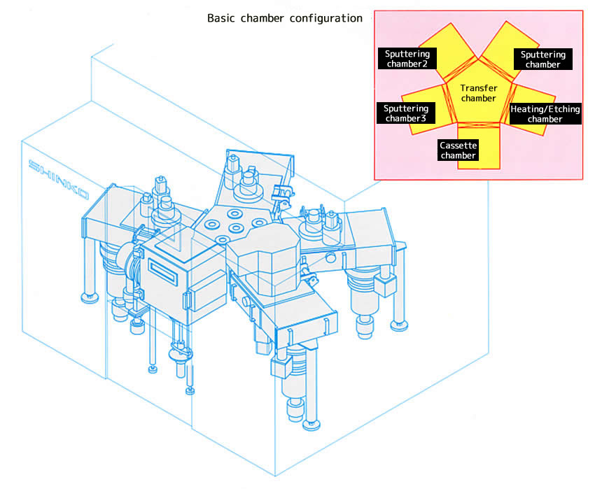
Multi-chamber sputtering system
This latest model of sputtering system can be flexibly applied to any type of substrate (Si wafer, glass, ceramics, etc.)
Owing to market-tested software and flexible hardware design, the multi-chamber sputtering system for R & D that was first released in 1991 has evolved into a full-fledged cluster tool that covers development, prototyping and production of cutting-edge devices.
As an integration of SHINKO SEIKI’s thin film forming technologies, the STM series has played an active role in various fields, including semiconductor, FPD, MEMS and state-of-the-art surface mounting processes.
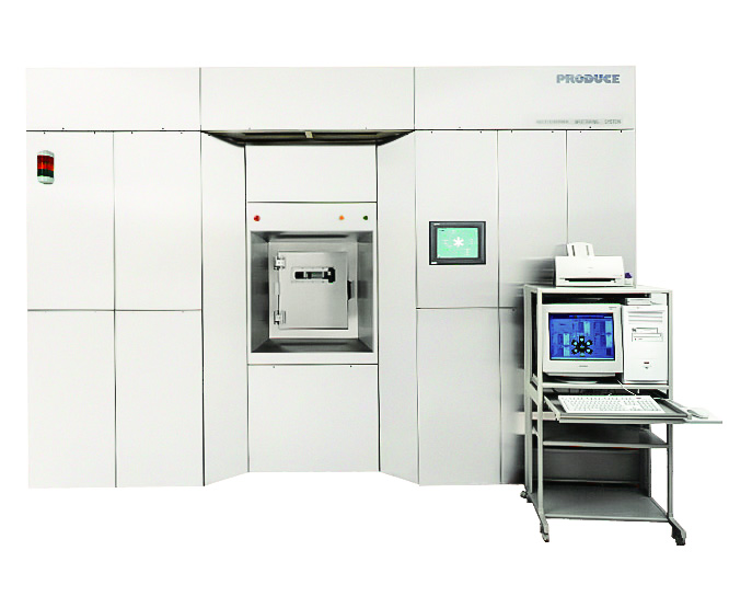 Model:STM4415
 [Features]
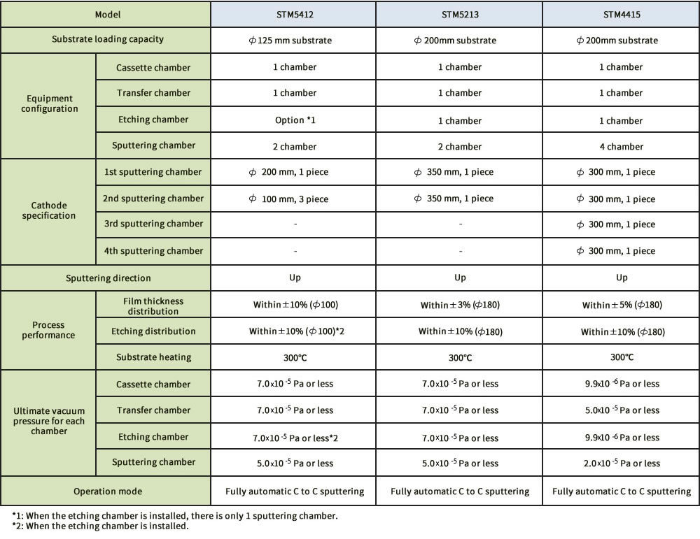
- The STM series enables processing of glass and ceramic panels of up to 203 mm diagonal, as well as wafer substrates (φ76.2 to φ203.2 mm).
- The STM series provides various selective functions so that it can be applied to basic research into future processing and various prototyping and production processes.
- The STM series is built with modular units, with emphasis placed on reliability.
- Maintenance can be performed separately on chambers, which both facilitates maintenance work and shortens maintenance and startup time.
- Having the space-saving design and through-wall structure, the STM series is applicable to high-level cleanrooms.
Equipment specifications
Basic chamber configuration